Description
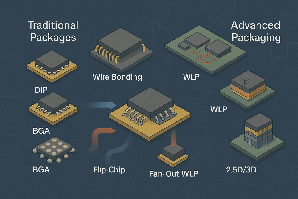
This intensive three-day program provides a deep dive into both Traditional Packaging Technologies—including DIP, QFP, BGA, Wire Bonding, and Flip-Chip—and cutting-edge Advanced Packaging Technologies such as System-in-Package (SiP), Wafer-Level Packaging (WLP), Fan-Out WLP, 2.5D/3D stacking, and Through-Silicon Via (TSV). Participants will gain hands-on insights into materials, processes, design considerations, and reliability challenges that underpin modern IC package development. Emphasis is placed on real-world applications in consumer, mobile, and high-performance devices, along with cost-performance trade-offs and manufacturing best practices.
Duration of Modules (24 Hours Total)
| Module | Topics Covered | Duration (hours) |
| Traditional Packaging | – Dual In-Line Packages (DIP): Structure & variants; manufacturing process; applications & limitations – Quad Flat Packages (QFP): Configurations; fine-pitch variants; assembly considerations – Ball Grid Array (BGA): Structure & advantages; fine-pitch, ceramic & plastic BGA variants | 4 |
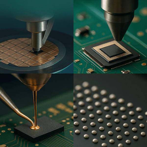
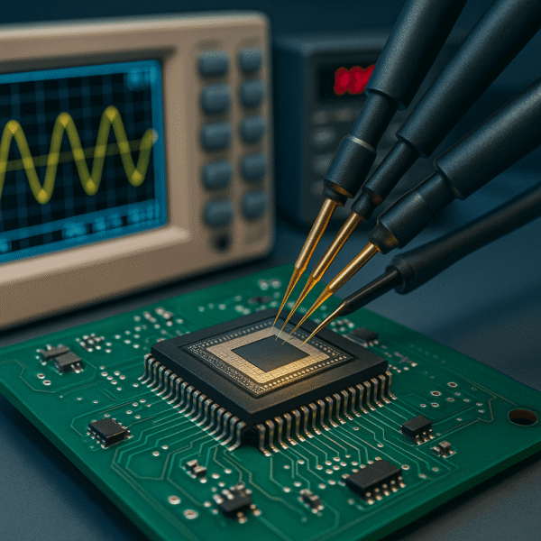
| Interconnect & Flip-Chip | – Wire Bonding: Ball vs. wedge bonding; materials & equipment; process optimization; QC & inspection – Flip-Chip: Controlled Collapse Chip Connection (C4); solder bump formation; underfill; module reliability | 4 |
| Advanced Packaging | – System-in-Package (SiP): Multi-chip integration; heterogeneous integration; design methodologies; mobile device applications – Wafer-Level Packaging (WLP): Chip-scale packaging; redistribution layer (RDL); process flow; cost & limitations – Fan-Out WLP: eWLB structure; process challenges; high-performance use cases – 2.5D/3D Stacking: TSV technology; die stacking; interposer-based designs; HBM integration; thermal/mechanical considerations; cost-performance trade-offs | 6 |
➢ Learning Outcomes
By the end of this course, participants will be able to:
- Select and design traditional IC packages (DIP, QFP, BGA) tailored to specific performance and cost requirements
- Understand key wire bonding and flip-chip interconnect processes, materials, and reliability strategies
- Apply principles of SiP, WLP, and Fan-Out WLP manufacturing, including redistribution layers (RDL) and eWLB techniques
- Implement techniques for 2.5D/3D stacking using TSVs and silicon interposers, focusing on high-bandwidth memory integration
- Analyze trade-offs among package cost, performance, thermal management, and mechanical reliability
- Employ best practices for process optimization, quality control, and failure analysis
➢ Target Audience
This course is designed for:
- Packaging engineers and designers seeking advanced knowledge of IC packaging technologies
- Process engineers responsible for assembly, reliability, and quality control in semiconductor manufacturing
- R&D professionals exploring heterogeneous and 3D integration solutions
- Product managers and system architects evaluating packaging options for next-generation electronic devices
- Graduate students and technical specialists aiming to deepen their understanding of both traditional and emerging packaging methodologies
➢ Skills You’ll Gain
- Mastery of wafer thinning and precision dicing techniques
- Selection and application of die-attach adhesives and eutectic systems
- Proficiency in wire bonding and flip-chip interconnect formation
- Understanding of flux cleaning and underfill process optimization
- Knowledge of encapsulation materials, molding methods, and laser marking
- Expertise in solder ball attachment and thermal profiling for reflow
- Operational competency with IC packaging equipment and cleanroom best practices
➢ Target Audience
This module is designed for:
- Packaging engineers and designers seeking advanced knowledge of IC packaging technologies
- Process engineers responsible for assembly, reliability, and quality control in semiconductor manufacturing
- R&D professionals exploring heterogeneous and 3D integration solutions
- Product managers and system architects evaluating packaging options for next-generation electronic devices
- Graduate students and technical specialists aiming to deepen their understanding of both traditional and emerging packaging methodologies
Reviews
There are no reviews yet.