Description
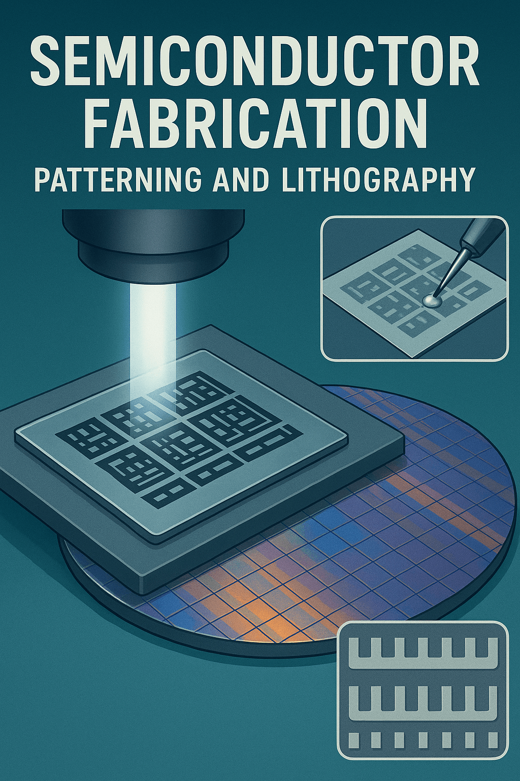
This course provides an in-depth exploration of the patterning and lithography processes fundamental to semiconductor device manufacturing. Building on foundational fabrication concepts, it covers the full spectrum of pattern transfer methods necessary for defining the intricate features of modern integrated circuits. Key topics include pre-patterning surface preparation, photoresist technologies, mask and reticle usage, various lithography techniques (such as contact, proximity, projection, deep UV, electron-beam, and nanoimprint), and methods for advanced patterning to achieve sub-micron and nanoscale device features.
➢ Course Objectives
- Explain the end-to-end patterning process and its criticality in device miniaturization.
- Select appropriate lithography methods for specific device requirements and technology nodes.
- Analyse the function of each component (resist, mask, exposure tool) in the lithography workflow.
- Troubleshoot and optimize patterning steps to enhance device performance and manufacturing yield.
➢ Time duration 4 to 4.5 hours
Reviews
There are no reviews yet.