Description
Module 1 provides a comprehensive overview of semiconductor packaging, covering its purpose, benefits, and historical evolution. Learners will explore the fundamentals of how packages protect, interconnect, and enable high-performance integrated circuits. Through real-world examples, you will understand why packaging is critical to reliability, thermal management, and system integration in modern electronics.
➢ What You’ll Learn
- Define semiconductor packaging and its core functions.
- Articulate the need for packaging, including protection, signal integrity, and thermal stewardship.
- Describe the packaging process flow, from substrate design through final inspection.
- Trace the history and evolution of packaging technologies, from DIP to 3D-ICs.
- Differentiate major packaging families and categories, such as through-hole, surface-mount, BGA, CSP, and advanced 2.5D/3D approaches.
➢ Skills You’ll Gain
- Clear understanding of packaging roles in modern devices.
- Ability to map out key manufacturing steps: die attach, underfill, wire bonding, solder balling, and testing.
- Familiarity with historical milestones that shaped package design.
- Competence in classifying packages by construction, application, and performance trade-offs.
- Foundation for evaluating package selection based on mechanical, thermal, and electrical criteria.
➢ Target Audience
Engineers, designers, and technicians seeking a solid introduction to semiconductor packaging, including:
- New graduates entering packaging or test engineering.
- Product‐development professionals requiring packaging insight.
- Manufacturing and quality engineers expanding into packaging processes.
- Anyone interested in the fundamentals of how packaging impacts device reliability and system integration.
➢ Topics Covered
- What Is Semiconductor Packaging?
- Definition and primary objectives
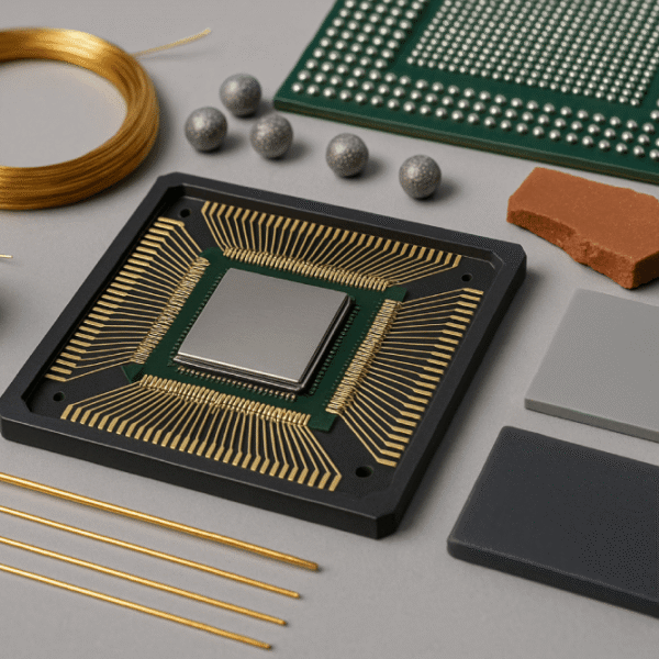
- Key components: die, substrate, interconnects, and enclosure - Need for Packaging
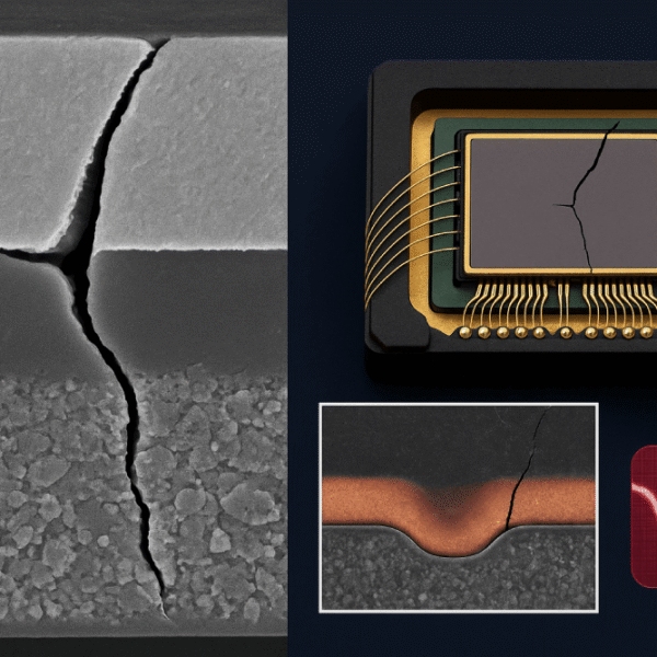
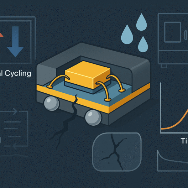
- Protecting silicon from mechanical and environmental damage
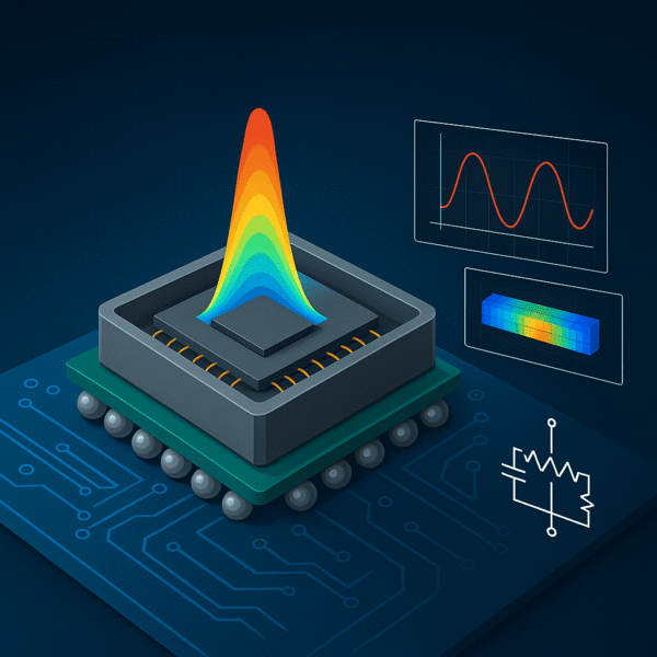
- Ensuring electrical connectivity and signal integrity
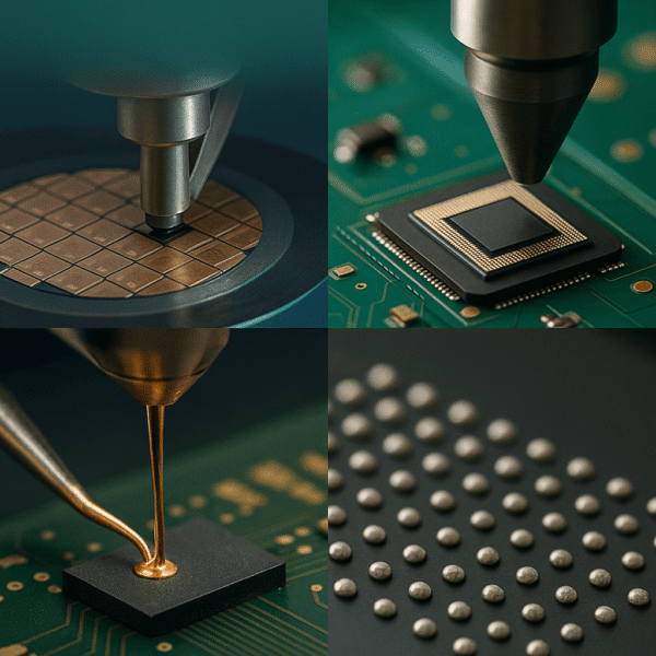
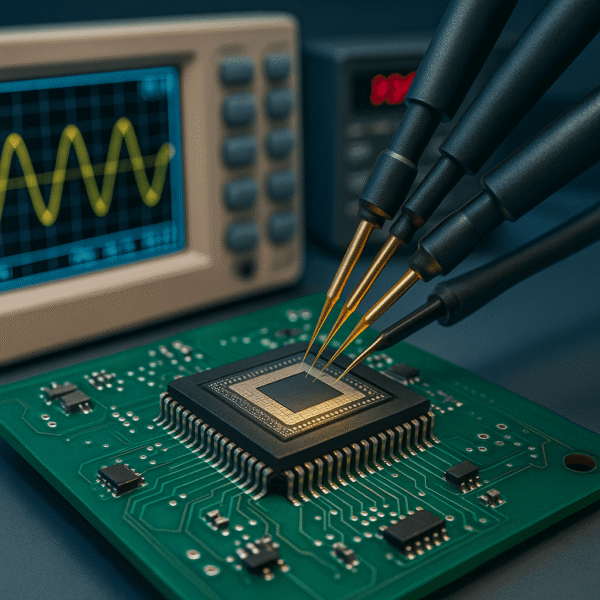
- Managing heat dissipation and reliability - Packaging Process Flow
- Substrate design and material selection
- Die attach and underfill
- Wire bonding vs. flip-chip interconnects
- Ball attach, molding, and curing
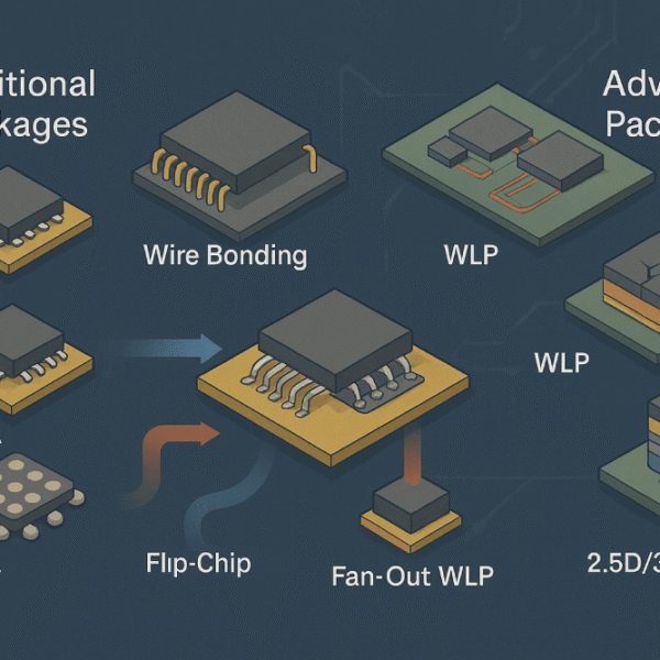
- Final test, inspection, and marking - History and Evolution of Packaging
- Early DIP and SIP packages
- Transition to surface-mount and BGA
- Emergence of chip-scale (CSP) and wafer-level packaging
- Advanced 2.5D, 3D-IC, and heterogeneous integration - Packaging Families and Categories
- Through-hole vs. surface-mount
- Ball Grid Array (BGA) vs. Land Grid Array (LGA)
- Chip-Scale Package (CSP) and Wafer-Level Package (WLP)
- Advanced multi-die and co-packaging solutions
➢ Time duration 4 hours
Reviews
There are no reviews yet.