Description
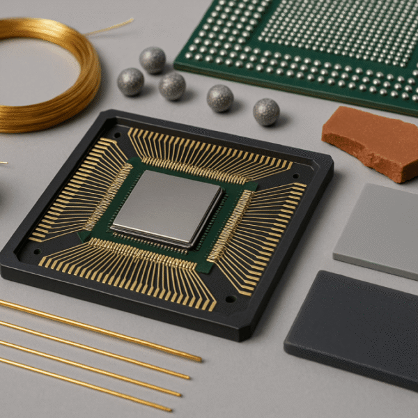
This intensive 5-hour course provides a comprehensive overview of advanced failure analysis and inspection techniques used in semiconductor packaging. Participants will learn how to apply key electrical, non-destructive, visual, and microscopic test methods—as well as automated inspection systems—to ensure package integrity, enhance yield, and troubleshoot defects effectively.
➢ Duration of Modules
| Module | Duration |
| 1 Electrical Testing | 1.5 Hours |
| 2 Non-Destructive Inspection | 1.5 Hours |
| 3 Visual Inspection Systems and Automated Failure Analysis | 0.75 Hour |
| 4 Failure Analysis Techniques | 1.25 Hours |
| Total | 5 Hours |
➢ Learning Outcomes
Upon completion of this course, participants will be able to:
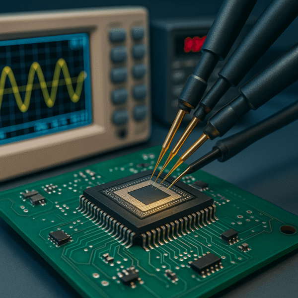
- Implement parametric and functional electrical tests to verify package performance.
- Utilize non-destructive X-ray, acoustic, and optical inspection methods for defect detection.
- Set up and operate visual inspection systems, leveraging AI-based anomaly detection.
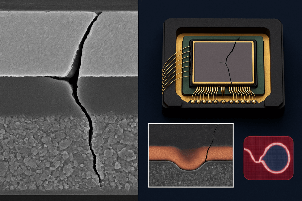
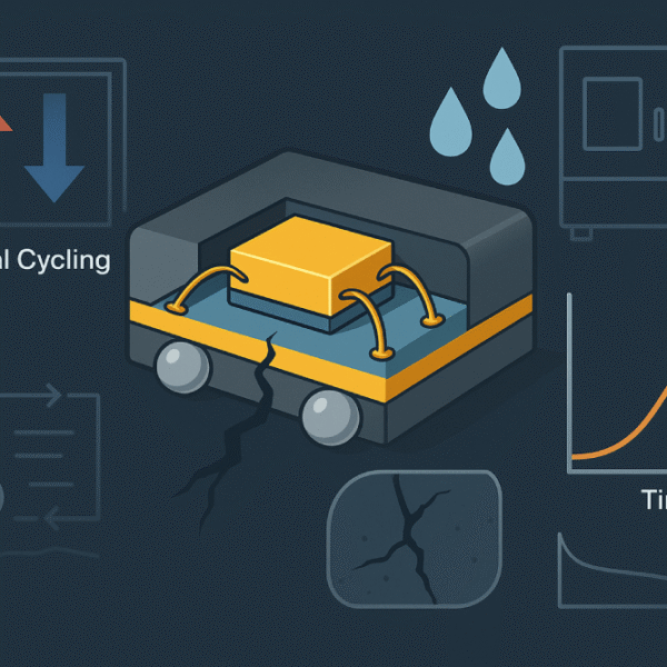
- Execute advanced failure-analysis workflows, including cross-sectional SEM, FIB-SEM, TEM, and decapsulation techniques.
- Analyze data using SPC and yield-mapping strategies to drive process improvements.
- Integrate inspection findings with manufacturing execution systems for real-time quality control.
➢ Target Audience
This course is designed for:
- Packaging engineers and process development engineers in semiconductor fabrication.
- Failure analysis specialists seeking advanced inspection and diagnostic skills.
- Quality and reliability engineers responsible for package integrity.
- R&D professionals and lab technicians working on semiconductor assembly and test.
- Managers overseeing yield enhancement, quality assurance, and failure-analysis teams.

Reviews
There are no reviews yet.