Description
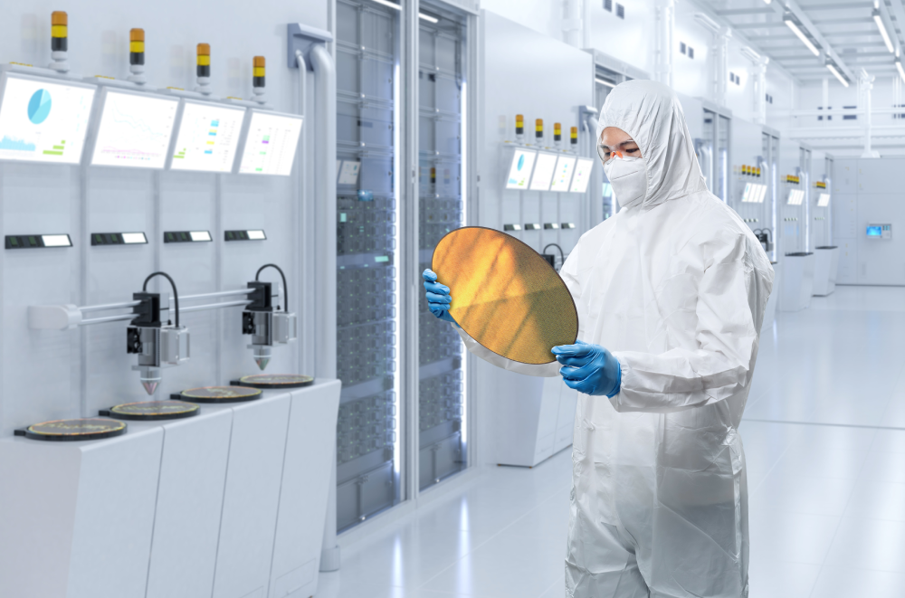
Semiconductor manufacturing is a sophisticated, multi-step process fundamental to modern electronics. This course provides an in-depth overview of two essential stages: silicon wafer fabrication and semiconductor deposition. The silicon wafer fabrication section covers methods such as single-crystal growth, wafer grinding, slicing, edge grinding, lapping, etching, and polishing, establishing the pristine foundation required for device manufacturing. The semiconductor deposition module introduces and compares the principal thin film deposition techniques—epitaxy, CVD, PVD, ALD, ECD, SOD—and explains their roles in forming functional device layers and patterns. Throughout the course, interactive quizzes reinforce learning and promote retention of visually rich, engaging content.
➢ Course Objectives
Describe the sequential steps in silicon wafer fabrication, including crystal growth, slicing, lapping, etching, and polishing.
Recognize the major types of epitaxy, and explain the processes involved in their creation.
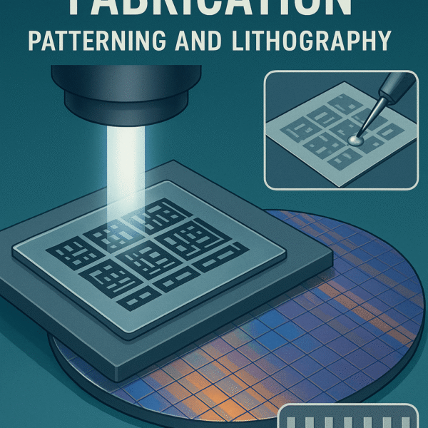
Identify and distinguish the various deposition techniques used for thin film and pattern formation on silicon wafers, noting the specific applications for each.
Explain the operating principles behind key deposition methods: Chemical Vapor Deposition (CVD), Physical Vapor Deposition (PVD), Atomic Layer Deposition (ALD), Electrochemical Deposition (ECD), and Spin-On Deposition (SOD).
➢ Time duration 3 to 3.5 hours
Reviews
There are no reviews yet.