Description
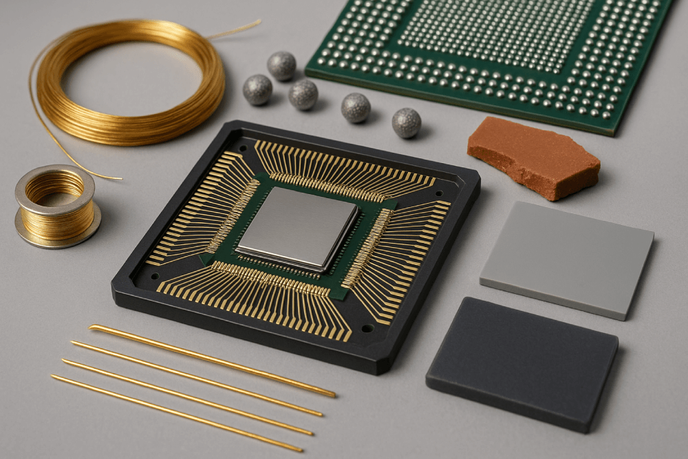
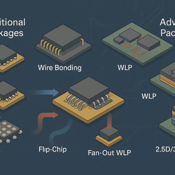
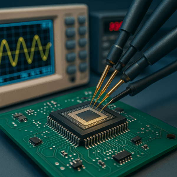
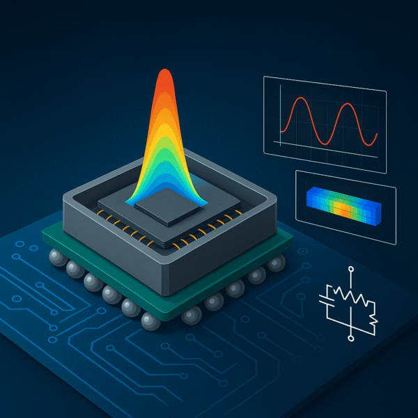
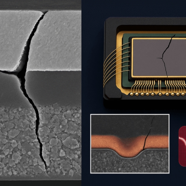
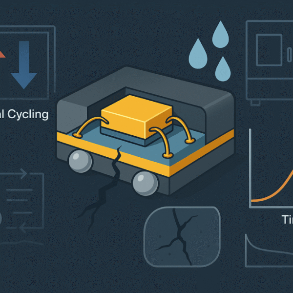
IC Packaging Metallurgy explores the foundational materials science and engineering concepts crucial to advanced IC packaging. The course covers the metallurgical aspects of key materials—including die-attach adhesives and solders, underfill compounds (epoxies and silicones), bonding wires, wafer-level bumping materials, under-bump metallurgy (UBM), and ceramic/glass substrates. Emphasis is placed on material’s selection, critical properties, processing challenges, failure mechanisms, and industry applications. Lectures are designed for practical engagement, integrating problem-solving and case studies relevant to the latest packaging technologies and reliability demands.
➢ Duration of Modules
| Module | Duration |
|---|---|
| Die-Attach Adhesives and Solders | 3 hours |
| Underfill Compounds (Epoxies, Silicones) | 2 hours |
| Bonding Wires (Materials, Diameters) | 2 hours |
| Wafer-Level Bumping Materials | 2 hours |
| Under-Bump Metallurgy (UBM) | 2 hours |
| Ceramic and Glass Substrates | 2 hours |
| Case Studies, Applications, Q & A | 2 hours |
| Total | 15 hours |
➢ Learning Outcomes
Participants completing this course will:
- Describe the structure, and selection criteria for major packaging materials (adhesives, solders, epoxies, wires, bumping materials, substrates).
- Assess the impact of material choices on mechanical, thermal, and electrical performance and long-term reliability of IC packages.
- Evaluate industry-relevant packaging processes, including die attach, wire-bonding, underfill dispensing, wafer bumping, and UBM stack assembly.
- Apply metallurgical knowledge to troubleshoot material-related failures and optimize package design for yield and reliability.
- Understand testing, inspection, and reliability assessment techniques for metallurgical interfaces in semiconductor packaging.
➢ Target Audience
This course is ideal for:
- Engineers and technicians working in IC packaging, semiconductor assembly, process and yield engineering.
- Materials scientists and researchers with an interest in electronic packaging metallurgy.
- Technical sales, procurement, and supply chain staff handling semiconductor materials.
- Quality, reliability, and failure analysts for electronics/devices.
- Upper-level students (graduates/advanced undergraduates) in microelectronics, metallurgy, or materials science.
- Professionals transitioning into the semiconductor industry or seeking upskilling for advanced packaging trend
Reviews
There are no reviews yet.