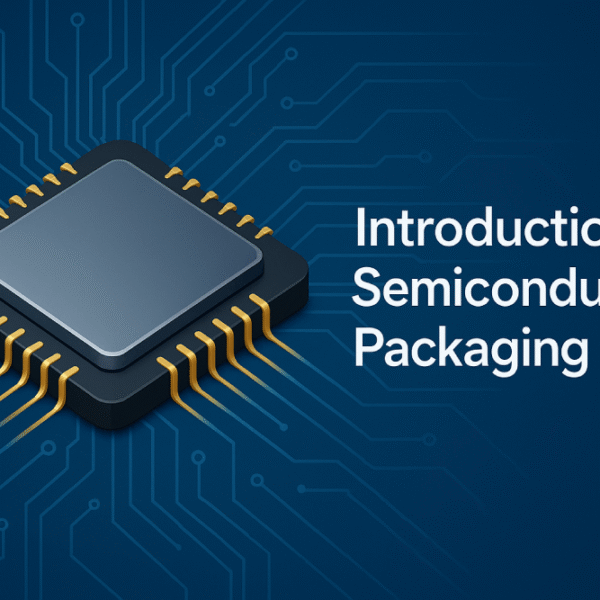
Description
This intensive 9-hour module delves into the critical manufacturing steps that transform a bare die into a fully encapsulated, ready-to-use semiconductor package. Participants will explore best-practice techniques—from wafer thinning and die singulation through advanced interconnect formation and final encapsulation—gaining hands-on insight into equipment, materials, and process controls essential for modern IC packaging operations.
➢ Curriculum Duration
Total Contact Hours: 9 hours
- A. Die Preparation (1.5 hrs)
– Wafer thinning
– Dicing and singulation - B. Die Attachment (1 hr)
– Die-attach adhesives
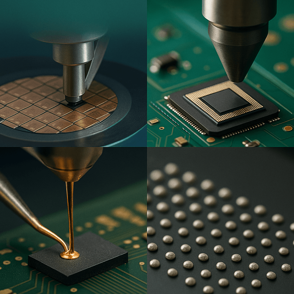
– Eutectic die-attach methods - C. Interconnect Formation (2.5 hrs)
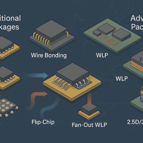
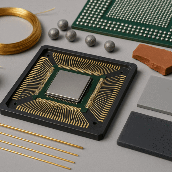
– Wire bonding (gold, aluminum)
– Flip-chip processes (solder bumping, under-bump metallurgy) - D. Cleaning and Underfill (1 hr)
– Flux cleaning techniques
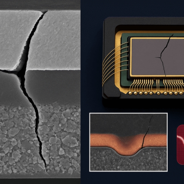
– Underfill materials and process - E. Encapsulation and Marking (1.5 hrs)
– Molding compounds and encapsulation methods
– Laser marking - F. Ball Attach and Reflow (1 hr)
– Solder ball attachment
– Reflow profiling - G. Equipment and Operations (1.5 hrs)
– IC packaging toolsets
– Cleanroom protocols and safety
➢ Skills You’ll Gain
- Mastery of wafer thinning and precision dicing techniques
- Selection and application of die-attach adhesives and eutectic systems
- Proficiency in wire bonding and flip-chip interconnect formation
- Understanding of flux cleaning and underfill process optimization
- Knowledge of encapsulation materials, molding methods, and laser marking
- Expertise in solder ball attachment and thermal profiling for reflow
- Operational competency with IC packaging equipment and cleanroom best practices
➢ Target Audience
This module is designed for:
- Process engineers and technicians in semiconductor packaging
- Manufacturing engineers seeking to optimize yield and reliability
- Quality engineers focused on package integrity and failure analysis
- R&D professionals developing advanced packaging solutions
- Cleanroom operations personnel and equipment maintenance staff
Participants will leave with both theoretical understanding and practical insights to implement robust, high-throughput packaging processes in production environments


Reviews
There are no reviews yet.